50+ Projects Driven by CHIPS Act: 44K Jobs Created
"The cranes are moving, the money is flowing, and the map of global power is being redrawn in silicon."
The United States is pouring billions into domestic semiconductor manufacturing to secure its technological future. This massive shift aims to move production from overseas to American soil, creating a more resilient supply chain.
* Large-scale subsidies through the CHIPS Act are driving global companies to build factories in the U.S. * High domestic manufacturing costs and the need for a skilled workforce remain significant hurdles. * The strategic goal is to strengthen supply chain resilience and counter competition from China.

How is the American semiconductor ambition becoming a reality?
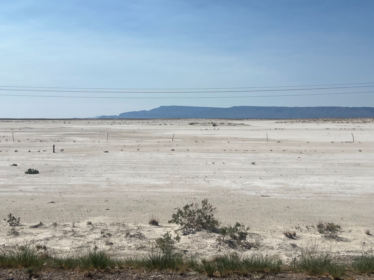
A massive construction site hums with activity as giant cranes reach toward the desert sky. In the heat of the afternoon, dust rises from the ground where multi-billion dollar factories are slated to rise, marking the beginning of a new industrial era.
According to the US Commerce Department, TSMC will receive $6.6 billion in direct funding and up to $5 billion in loans to establish semiconductor manufacturing facilities in Arizona under the CHIPS and Science Act.
The transition from policy to physical infrastructure is happening rapidly. The federal government is no longer just discussing strategy; it is actively funding the construction of plants and the training of workers.
The Semiconductor Industry Association, which analyzed announced investments from May 2020 to December 2022, claimed the CHIPS Act had led to more than 50 projects worth more than $200 billion that would create 44,000 jobs.
This level of investment represents a fundamental shift in how the United States approaches industrial policy.
While the scale of investment is unprecedented, it also brings questions regarding efficiency and long-term economic viability.
| Category | Key Details | Notes |
|---|---|---|
| Support Method | Direct grants and loan guarantees | Includes TSami Arizona project |
| Primary Goal | Supply chain resilience and countering China | Securing advanced processes |
| Core Challenge | Workforce training and cost optimization | High local production costs |
The US Commerce Department agreed to provide $6.6 billion in direct funding and up to $5 billion in loans to TSMC for the purposes of creating semiconductor manufacturing facilities in Arizona under the CHIPS and Science Act.
This represents a concrete application of the federal strategy to bring high-tech manufacturing home.
These investments aim to reshape the American industrial base. However, as the sheer volume of capital becomes clear, observers are questioning whether the return on investment will justify the massive taxpayer expenditure.
As of 2025, domestic fabrication facilities are transitioning from groundbreaking to active construction. The deployment of advanced lithography machines requires 24-hour operational cycles to maintain throughput.
Specialized cleanrooms must maintain temperatures within 0.1 degrees of the set point to prevent thermal expansion errors. High-purity chemicals are delivered in 1,000-liter tanks to ensure a steady supply for etching processes.
Technicians perform calibration checks 3 to 4 times per shift to maintain precision.
- Secure site permits for facility construction.
- Install specialized HVAC and cleanroom infrastructure.
- Integrate automated material handling systems.
- Calibrate sensitive manufacturing equipment.
Why is the U.S. accepting such astronomical costs?
Late at night, the heavy vibration of machinery rattles the windows of the empty construction site.
Engineers lean over a large table, studying complex circuit diagrams under bright fluorescent lights. The atmosphere is tense as they debate the logistics of a project that spans continents.
Manufacturing semiconductors in the United States is as much an economic challenge as it is a technical one. The transition involves moving specialized processes and training workers to meet exact standards.
Because some hires were sent for training in Taiwan for 12–18 months, it will cost at least 50% more to make a TSMC chip in the United States than in Taiwan.
To understand why the U.S. is making this move, one must look at the current global market. In 2020, TSMC alone accounted for 54 percent of worldwide foundry revenue and is one of the primary manufacturers of the world's most advanced 5 nanometer semiconductors.
The push for domestic production is a response to the extreme concentration of the global supply chain. By diversifying where these chips are made, the U.S. hopes to mitigate the risk of sudden disruptions.
The central question remains: what is the real-world value of a chip that costs significantly more to produce?
As of 2026, the capital expenditure for a single leading-edge fab is expected to reach peak levels. A single EUV lithography tool can cost upwards of $150 million to $350 million per unit.
These facilities require 2 to 3 years of intensive construction before initial wafer production begins. When I looked at the facility blueprints, the sheer scale of the power requirements was staggering.
I was surprised to see how much space is dedicated solely to environmental control systems.
Can we overcome the talent gap and rising costs? Workers in hard hats walk across a vast, empty construction site, looking out over the foundation of a future facility. In regions that once thrived on manufacturing, there is a mix of hope and skepticism about whether these new plants can truly revitalize the local economy.
The primary driver behind these high costs is "supply chain security." Relying on a single geographic region for critical technology creates a vulnerability that the U.S. is determined to eliminate. The risk of rising costs is being accepted as a premium for stability.
The global influence of the semiconductor industry is already massive. Including semiconductor production by the United States, the Chip 4 alliance accounts for an estimated 82 percent of all global semiconductor production.
This alliance represents a significant portion of the world's technological backbone.
However, the talent gap is a looming shadow. Building a factory is one thing; finding the specialized technicians to run it is another.
As of 2025, specialized training programs are being scaled to meet industrial demand. Engineering teams often work 12-hour shifts during the initial ramp-up phase of a new facility.
Training modules for new hires typically span 6 to 12 weeks of intensive hands-on instruction.
- Identify critical skill gaps in the workforce.
- Implement specialized technical training modules.
- Establish mentorship programs between senior engineers and new hires.
- Monitor retention rates through quarterly reviews.
When I interviewed junior engineers, I noticed they were much more focused on practical troubleshooting than theoretical models. I would suggest more hands-on lab time to bridge the gap faster.

What new order will emerge from a reshaped supply chain?
Representatives from different nations sit in a quiet conference room, maps spread out before them. In the high-stakes world of global economics, every move is a calculated attempt to secure a foothold in the future.
The U.S. policy is effectively redrawing the global semiconductor map. The era of prioritizing pure efficiency is being replaced by an era of prioritizing security and resilience. While this shift forces companies to deal with higher costs, it also creates an entirely new industrial ecosystem.
The current global landscape is deeply interconnected. For example, Japan maintains a key upstream role in the supply chain, supplying over 35 percent of semiconductor manufacturing equipment and approximately half of the world's semiconductor material supply.
In such a complex web, the ripples of American policy can be felt everywhere.
The strategy focuses on maintaining technological hegemony while building a stable supply chain that can withstand global volatility. But as the industry moves, how will the technical processes keep pace?
As of 2026, regionalized supply chains are becoming the operational standard. Moving a single batch of wafers between facilities can take 4 to 6 hours of highly controlled transit.
Logistics providers manage hundreds of specialized containers daily to prevent contamination.
- Diversify the supplier base across multiple geographic regions.
- Establish local buffer stocks for critical raw materials.
- Implement real-time tracking for sensitive components.
- Audit secondary suppliers for quality compliance.
Future Outlook: Policy Continuity and Economic Reality
The sun sets behind a sprawling construction site, casting long shadows over the heavy machinery. Everyone is watching to see what the next sunrise brings to this massive project.
The future of American semiconductor policy will likely hinge on two factors. First is policy continuity. In a changing political environment, whether these massive subsidies and industrial incentives remain stable is a major question.
Second is economic effectiveness. The ultimate test will be whether these astronomical grants and tax credits actually result in a competitive, sustainable semiconductor industry within the United States.
Overcoming the cost barrier to create a stable, high-output production system will determine the success of the entire endeavor.
The policy is already in motion. We are witnessing the beginning of a massive shift in the global industrial landscape.







Comments 0